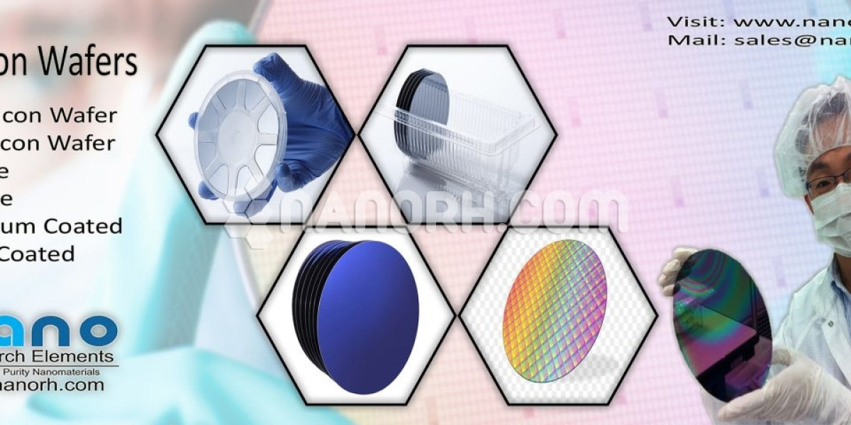
Silicon is a significant element that has become an integral part of our daily lives, and it is used in the form of various appliances and applications. This is the second most ample element on earth, and it has unique properties. This element is the foundation of the electronic and technological sectors. Let us delve deep into this topic by reading this article to learn what silicon wafers are exactly and what their importance is.
A precise idea of silicon wafers
Silicon is the most widely used semiconductor in electronic devices. It is a thin, flat material that delivers itself as the substrate for the fabrication of microchips and integrated circuits. These wafers are typically ultra-thin, varying from micrometers to numerous millimeters in thickness. Silicon wafers are usually used as base sheets or ground layers for constructing complex circuit designs. Due to its extraordinary electrical properties, it becomes ideal for the manufacturing of semiconductors. It acts as a platform where various material processes take place to construct and create the micro-components essential for electronic devices.
To make a silicon wafer, various kinds of extraction and purification are done from the raw silicon. The raw silicon is melted in a crucible and is then drawn out using a seed crystal.
A large chunk of silicon is drawn out, also known as an ingot, and once grown, is sliced into thin disks using wire saws. The purity of silicon wafers is vital for its optimum usage. These disks become silicon wafers. The thickness often varies depending on their usage. After slicing these disks, the wafers are polished and cleaned.
The silicon wafers are made to go through various processes to become suitable and useful for their intended purposes. Doping is a process in which impurities are deliberately added to the silicon wafers to modify their electrical properties. This allows the silicon wafer to behave as negative and positive semiconductors necessary for the functionality of transistors and two terminal electrical devices.
Various shapes and sizes
As mentioned earlier, silicon wafers come in various forms depending on their intended usage. Some of its types are monocrystalline wafers, silicon insulators, and polycrystalline wafers.
These various types of silicon are used in several industries, from microchips and integrated circuits in mobile and computers to solar cells, medical devices, and quantum computing; silicon wafers are the unsung heroes of modern technologies.
In the manufacturing of silicon wafers, ethyl silicate principally comes into the picture. While the deposition of ultrathin silica films takes place, ethyl silicate primarily contributes to the fabrication process of wafers. This organic silicon compound is also used in the Sol-Gel process, another procedure for making silicon wafers. In this process, ethyl silicate undergoes hydrolysis and polycondensation to form a gel-like substance, which is used as an anti-reflective to coat silicon wafers. The inclusion of ethyl silicate in the silicon wafer heightens its purity, versatility, and stability.


