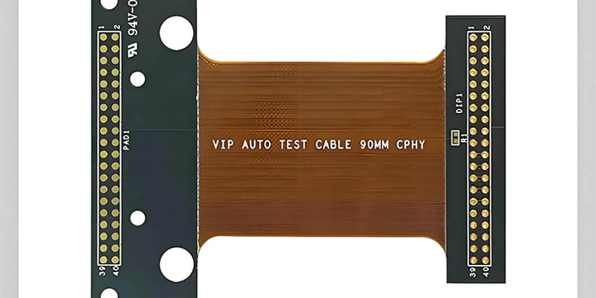
Understanding Rigid-Flex PCBs
Rigid-Flex PCBs are a type of printed circuit board where rigid circuit substrates and flexible circuit substrates are laminated together. This combination allows for the mounting of components on the rigid sections while using the flexible parts to replace wired connections. The rigid sections function like traditional rigid PCBs, where components can be soldered on both sides, and multilayer connections can be made. Meanwhile, the flexible parts can connect multiple layers but are not typically used for component mounting, as their primary role is to facilitate connections between the rigid sections.
Eliminating connectors in the design introduces several benefits to the circuit:
Signal Integrity: There is no loss or jitter (noise) in signal transmission between sections.
Reliability: Eliminates issues related to cold joints and other connector problems.
Space and Weight Efficiency: Frees up space and reduces overall weight.
Durability: This makes the circuit vibration-resistant and suitable for applications with moving parts.
Designing pcb flex rigid
Designing a Rigid-Flex PCB requires specialized software, and the key consideration is selecting the appropriate copper trace width based on the application.
Trace Width Calculation:
\[ \text{Width} = \frac{\text{Area}}{\text{Thickness} \times 1.378} \]
For internal layers, use a constant \( k = 0.024 \), and for external layers, use \( k = 0.048 \).
Gekunflex engineers are available to guide you in selecting the correct trace width and optimal materials based on your operational frequency and application needs.
Simulating Flexible PCBs
Early simulation practices can help designers prevent numerous errors by revealing issues related to bending. This saves both time and money by allowing designers to predict bending radii and choose the correct copper trace orientation to prevent tearing or discontinuity.
Designing with Offset Copper Traces
Incorporating additional copper into the design can enhance the dimensional stability of flexible circuits. For single-layer and double-sided flexible designs, offsetting the copper around the traces is a beneficial practice. Whether to add or remove extra copper depends on the application, but designs with offset traces should be prioritized for mechanical stability. Moreover, this approach reduces the amount of copper etched away, making it environmentally friendly from a chemical use perspective.
Binder Construction in Multilayer Flex
To facilitate multilayer flexible circuit design, an interleaved length design is typically used. In this technique, designers slightly increase the length of each subsequent flexible layer, typically by 1.5 times the thickness of a single layer. This method prevents bending stress from focusing on the center of the layers in multilayer flexible circuits, a critical consideration for dynamic applications.
Trace Routing at Corners
In flexible circuits, trace routing at corners should be done with care to avoid issues such as increased layer count and higher costs. The traces should be routed by bending and folding at the corners rather than using sharp angles, as sharp angles can trap the etching solution and may lead to over-etching, making post-processing cleanup difficult. When copper traces are present on both sides of the flexible circuit, designers should maintain a space of 2-2.5 times the trace width to prevent electrical shorts and ensure proper etching. Following these guidelines improves signal propagation and reduces reflections at bends.
Rigid-to-Flex Transition Zones
The minimum distance from the transition zone between rigid and flexible areas to the edges of clearance holes and plated-through holes should be no less than 0.0748 inches. In designs with non-plated through-holes and cutouts, the distance between the inner and outer edges should leave no less than 0.0197 inches of remaining material.
Plated Through-Holes at the Rigid-Flex Interface
It is recommended that the minimum distance between plated through-holes in the rigid section and the rigid-flex interface exceed 0.125 inches. Failure to adhere to this guideline may compromise the reliability of the plated through-holes.
Gekunflex's highly qualified engineers are always ready to provide guidance on design standards and validate the effectiveness of circuits in Rigid-Flex designs.
Conclusion
Designing PCB flex-rigid is a complex but rewarding task, offering numerous advantages in modern electronics. By following the proper guidelines for trace width, material selection, and layout, engineers can ensure the reliability and efficiency of their designs. Gekunflex's expertise in Rigid-Flex PCB technology can provide valuable support throughout the design process, ensuring optimal performance for your applications.